
Have you ever had that feeling when someone mentions anything at work or a social setting, and you’re like, “Hm, sounds interesting!” You know that moment when you know you’ve heard the term before, but you don’t have a good understanding of what it actually is. Yeah…. That’s FPGA for me (or at least, it used to be).

That acronym has been thrown at me so many times in the past year that I took upon myself to figure out, what it is? How does it work? What can I do with it? I am a hands-on learner. I need to understand the process, design and functionality of things from beginning to end, so I can sleep better at night and be better at my job. So, in this blog I am going to dive into FPGA for beginners, go over the basic structure, programming language and then… let’s see if I can do something simple with it.

What is an FPGA?
A Field Programmable Gate Array (FPGA) is a versatile device that allows users to configure and execute specific logic tasks by defining hardware functionality after it has been manufactured. Unlike traditional micro-controllers, FPGAs can be programmed and reprogrammed multiple times on the fly, allowing this flexibility to be a great benefit when changes are needed.
The flexibility that FPGAs provides is a significant advantage, to the performing of tasks requiring high processing power, speed, and parallelism—capabilities that micro-controllers cannot match. The FPGA’s parallel processing capability is essential for operations that demand high performance, efficiency, and flexibility.
Having a general understanding of the cyber threat landscape is important for us cybersecurity professionals. Understanding how FPGAs could help and impact the way we implement cyber resiliency in our critical systems is important. FPGAs flexibility of reprogramming allows a faster way to update security standards and mitigate risks.
Programming Languages
There are two main languages used to work with FPGAs: Verilog and VHDL (VHSIC Hardware Description Language). These are Hardware Description Languages (HDLs) which are used for designing and describing the structure and behavior of the digital logic circuits. Meaning that the FPGA will be working and interacting directly with the wires, logic gates and resources on the FPGA. That level of power does not happen with traditional programming languages like Python or C++.
There are some differences when it comes down to these programming languages that needs to be noted:
- Verilog looks like C, easier for people to read however it is case sensitive and this might create some issues that could be difficult to identify.
- VHDL is more widely used, is not case sensitive, although it requires more typing due to be more verbose, and it might be a bit difficult to read, but it reduces the likelihood of errors.
Verilog example:
module AndGate (input A, B, output Y);
    assign Y = A & B;
endmodule
VHDL example:
library IEEE;
use IEEE.STD_LOGIC_1164.ALL;

entity AndGate is
    Port (
        A : in STD_LOGIC; -- Input A
        B : in STD_LOGIC; -- Input B
        Y : out STD_LOGIC -- Output Y
    );
end AndGate;
NOTE: For this blog, all the code will be written in VHDL.
Hardware and Software
For this blog, I’ll be using the Nandland Go Board (more info here) and the iCEcube2 software from Lattice Semiconductor. iCEcube2 translates my VHDL code into a file that the FPGA can use for programming. Additionally, I’ll use the Diamond Programmer to upload the generated file to the FPGA via USB.
How to Build an FPGA Project
There are four steps to get my FPGA project up and running. These are: Design, Synthesis, Place and Route, and Programming
- Design: at this stage I write the VHDL code to define how the FPGA will function. Essentially, it’s where I decide the logic and behavior of my project.
- Synthesis: here, the VHDL code is translated into low-level components that the FPGA hardware can understand and use to perform the desired functions.
- Place and Route: here, the synthesized design is mapped to the physical FPGA layout. This process determines how signals in the code connect to FPGA pins and internal components.
- Programming: Finally, the result of the previous steps is loaded onto the FPGA through a programming file. This step configures the connections and makes the FPGA ready to execute the design.
Now, all I needed to do was figure out what I wanted to create with all this knowledge!

Hello, Let There Be Light!
Once my board came in, I was excited like a kid on Christmas day and… I just looked at it. You know that intense stared you give at something waiting to see if it will say something back at you or if the lightbulb in your head will ever come one? Yeah.. that feeling. I knew my intention was to get familiar with the programming concepts overall, so I decided to start with something simple. I wanted to see if I could program the board to when I press a switch all the LED lights will come on. And then it happened… I needed schematics!
Schematics
For me to know where to begin, I needed to understand how it connects! I found a schematic for the board online which provided detailed information about the LEDs, Switches and Connectors. Having this information is important since it will help me understand what information I needed for the VHDL code and mapping.
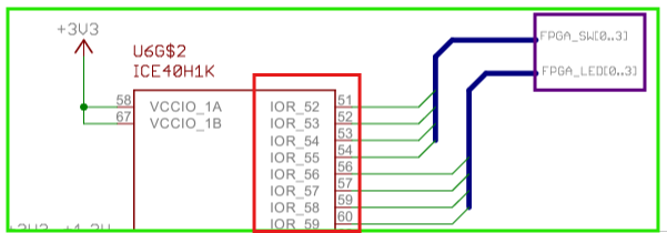
The schematic image shown below provide three important pieces of information that I need to take in consideration when programming my board. Within the red box is the Input/Output Resources (IOR) corresponding to the physical pins under the purple box, the Switches and the LEDs.
As I went through the schematics, I saw the information on the 2 digit 7-segment display! So, I decided why not use it! I decided to have the display to spell “HELLO” when I press the switch.
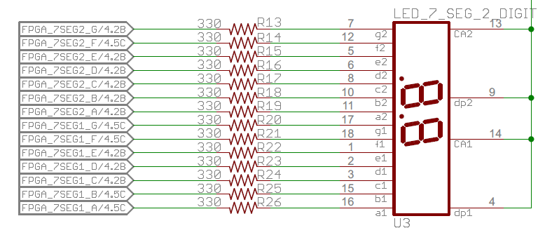
The schematic shown below covers a 2 digit segment display that comes with the board and how each segments are assigned.
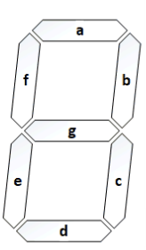
To ensure I programmed the segments correctly, I need to see what segment belong to what section on the display. I used the diagram below to help me identify the correct segments for each letter on HELLO.
Once I identify the segments I need for the letter, I use the following chart to assign bit value of the segment I need to be on or off, which then will provide me a binary pattern that will be added to the VHDL code.
| Segment | Active? | Bit Value |
|---|---|---|
| a | Yes/No | 1/0 |
| b | Yes/No | 1/0 |
| c | Yes/No | 1/0 |
| d | Yes/No | 1/0 |
| e | Yes/No | 1/0 |
| f | Yes/No | 1/0 |
| g | Yes/No | 1/0 |
VHDL Code
After a lot of trial and error, I created the following VHDL code to:
- Assign the input to Switch_1 that will control the blinking and the both 7 segment displays
- Set the output for the 7-Segment Displays 1 & 2
- It then sets the binary values of the letters in the word “HELLO”
- Process for 7-segment display character sequence
- It sets the blinking signal for the LEDs
library ieee;
use ieee.std_logic_1164.all;
use ieee.numeric_std.all;

entity Switches_To_Displays is
    port (
        clk          : in std_logic;       -- Clock
        reset        : in std_logic;       -- Reset
        i_Switch_1   : in std_logic;       -- Main switch to control blinking and 7-segment display
        o_LED_1      : out std_logic;      -- LED light 1
        o_LED_2      : out std_logic;      -- LED light 2
        o_LED_3      : out std_logic;      -- LED light 3
        o_LED_4      : out std_logic;      -- LED light 4
        o_Segment1_A : out std_logic;      -- Segments for Display 1
        o_Segment1_B : out std_logic;
        o_Segment1_C : out std_logic;
        o_Segment1_D : out std_logic;
        o_Segment1_E : out std_logic;
        o_Segment1_F : out std_logic;
        o_Segment1_G : out std_logic;
        o_Segment2_A : out std_logic;      -- Segments for Display 2
        o_Segment2_B : out std_logic;
        o_Segment2_C : out std_logic;
        o_Segment2_D : out std_logic;
        o_Segment2_E : out std_logic;
        o_Segment2_F : out std_logic;
        o_Segment2_G : out std_logic
    );
end entity Switches_To_Displays;

architecture Behavioral of Switches_To_Displays is
    -- Segment patterns and binary values for "HELLO"
    constant H_SEG : std_logic_vector(6 downto 0) := "0110111"; -- H
    constant E_SEG : std_logic_vector(6 downto 0) := "1001111"; -- E
    constant L_SEG : std_logic_vector(6 downto 0) := "0001110"; -- L
    constant O_SEG : std_logic_vector(6 downto 0) := "1111110"; -- O

    signal blink      : std_logic := '0'; -- Blinking signal for LEDs
    signal led_counter : unsigned(23 downto 0) := (others => '0'); -- Counter for LED blinking
    signal seg_counter : unsigned(50 downto 0) := (others => '0'); -- Counter for 7-segment display
    signal char_index : integer range 0 to 4 := 0; -- Index to track the character (H, E, L, L, O)
begin

    -- Process for LED blinking
    process(clk, reset)
    begin
        if reset = '1' then
            led_counter <= (others => '0');
            blink <= '0';
        elsif rising_edge(clk) then
            led_counter <= led_counter + 1;
            if led_counter = 0 then
                blink <= not blink;
            end if;
        end if;
    end process;

    -- Assign LEDs to blink when Switch 1 is pressed
    o_LED_1 <= blink when i_Switch_1 = '1' else '0';
    o_LED_2 <= blink when i_Switch_1 = '1' else '0';
    o_LED_3 <= blink when i_Switch_1 = '1' else '0';
    o_LED_4 <= blink when i_Switch_1 = '1' else '0';

    -- Process for 7-segment display character sequence
    process(clk, reset)
    begin
        if reset = '1' then
            seg_counter <= (others => '0');
            char_index <= 0;
        elsif rising_edge(clk) then
            if i_Switch_1 = '1' then
                seg_counter <= seg_counter + 1;
                if seg_counter = 5_000_000 - 1 then
                    seg_counter <= (others => '0');
                    char_index <= (char_index + 1) mod 5; -- Cycle through 0 to 4
                end if;
            else
                seg_counter <= (others => '0');
                char_index <= 0;
            end if;
        end if;
    end process;

    -- Assign segment patterns based on char_index and switch state
    process(char_index, i_Switch_1)
    begin
        if i_Switch_1 = '1' then
            case char_index is
                when 0 => -- Display "H" and "E"
                    o_Segment1_A <= not H_SEG(6);
                    o_Segment1_B <= not H_SEG(5);
                    o_Segment1_C <= not H_SEG(4);
                    o_Segment1_D <= not H_SEG(3);
                    o_Segment1_E <= not H_SEG(2);
                    o_Segment1_F <= not H_SEG(1);
                    o_Segment1_G <= not H_SEG(0);

                    o_Segment2_A <= not E_SEG(6);
                    o_Segment2_B <= not E_SEG(5);
                    o_Segment2_C <= not E_SEG(4);
                    o_Segment2_D <= not E_SEG(3);
                    o_Segment2_E <= not E_SEG(2);
                    o_Segment2_F <= not E_SEG(1);
                    o_Segment2_G <= not E_SEG(0);
                when 1 => -- Display "L" and "L"
                    o_Segment1_A <= not L_SEG(6);
                    o_Segment1_B <= not L_SEG(5);
                    o_Segment1_C <= not L_SEG(4);
                    o_Segment1_D <= not L_SEG(3);
                    o_Segment1_E <= not L_SEG(2);
                    o_Segment1_F <= not L_SEG(1);
                    o_Segment1_G <= not L_SEG(0);

                    o_Segment2_A <= not L_SEG(6);
                    o_Segment2_B <= not L_SEG(5);
                    o_Segment2_C <= not L_SEG(4);
                    o_Segment2_D <= not L_SEG(3);
                    o_Segment2_E <= not L_SEG(2);
                    o_Segment2_F <= not L_SEG(1);
                    o_Segment2_G <= not L_SEG(0);
                when 2 => -- Display "O" and blank
                    o_Segment1_A <= not O_SEG(6);
                    o_Segment1_B <= not O_SEG(5);
                    o_Segment1_C <= not O_SEG(4);
                    o_Segment1_D <= not O_SEG(3);
                    o_Segment1_E <= not O_SEG(2);
                    o_Segment1_F <= not O_SEG(1);
                    o_Segment1_G <= not O_SEG(0);

                    o_Segment2_A <= '1';
                    o_Segment2_B <= '1';
                    o_Segment2_C <= '1';
                    o_Segment2_D <= '1';
                    o_Segment2_E <= '1';
                    o_Segment2_F <= '1';
                    o_Segment2_G <= '1';
                when others =>
                    o_Segment1_A <= '1';
                    o_Segment1_B <= '1';
                    o_Segment1_C <= '1';
                    o_Segment1_D <= '1';
                    o_Segment1_E <= '1';
                    o_Segment1_F <= '1';
                    o_Segment1_G <= '1';

                    o_Segment2_A <= '1';
                    o_Segment2_B <= '1';
                    o_Segment2_C <= '1';
                    o_Segment2_D <= '1';
                    o_Segment2_E <= '1';
                    o_Segment2_F <= '1';
                    o_Segment2_G <= '1';
            end case;
        else
            -- Default to blank displays
            o_Segment1_A <= '1';
            o_Segment1_B <= '1';
            o_Segment1_C <= '1';
            o_Segment1_D <= '1';
            o_Segment1_E <= '1';
            o_Segment1_F <= '1';
            o_Segment1_G <= '1';

            o_Segment2_A <= '1';
            o_Segment2_B <= '1';
            o_Segment2_C <= '1';
            o_Segment2_D <= '1';
            o_Segment2_E <= '1';
            o_Segment2_F <= '1';
            o_Segment2_G <= '1';
        end if;
    end process;

end Behavioral;
Constraint Files
Now, that I have the VHDL code created, I needed to map the logical signals of my design to the physical pins of the FPGA. This will make the connection between the code and the hardware.
Within the code below is the the pin assignments for the following:
- Clock
- Switch
- 7-Segment Display 1 and 2
- LEDs
# FPGA Clock
set_io clk 15

# Switch
set_io i_Switch_1 53

# Segment Outputs
set_io o_Segment1_A 3
set_io o_Segment1_B 4
set_io o_Segment1_C 93
set_io o_Segment1_D 91
set_io o_Segment1_E 90
set_io o_Segment1_F 1
set_io o_Segment1_G 2
set_io o_Segment2_A 100
set_io o_Segment2_B 99
set_io o_Segment2_C 97
set_io o_Segment2_D 95
set_io o_Segment2_E 94
set_io o_Segment2_F 8
set_io o_Segment2_G 96

# Output LEDs
set_io o_LED_1 56
set_io o_LED_2 57
set_io o_LED_3 59
set_io o_LED_4 60
Programming
Now that I have my program written, I’ll need to import this to iCEcube2. iCEcube2 is an Integrated Development Environment or IDE, designed for working with Lattice Semiconductor’s. Here is where I can design, synthesize, place and route, and program FPGA projects in to the board.
Instructions:
- Open iCEcube2 and select File New Project.
- Name the project
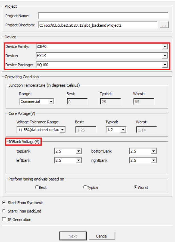
- Go to the Device section and select the following:
- Device Family- select iCE40
- Device- select HX1k
- Device Package – VQ100
- Change all IO Bank Voltage to 3.3
- Hit Next
- On the next screen I’ll add the VHDL file
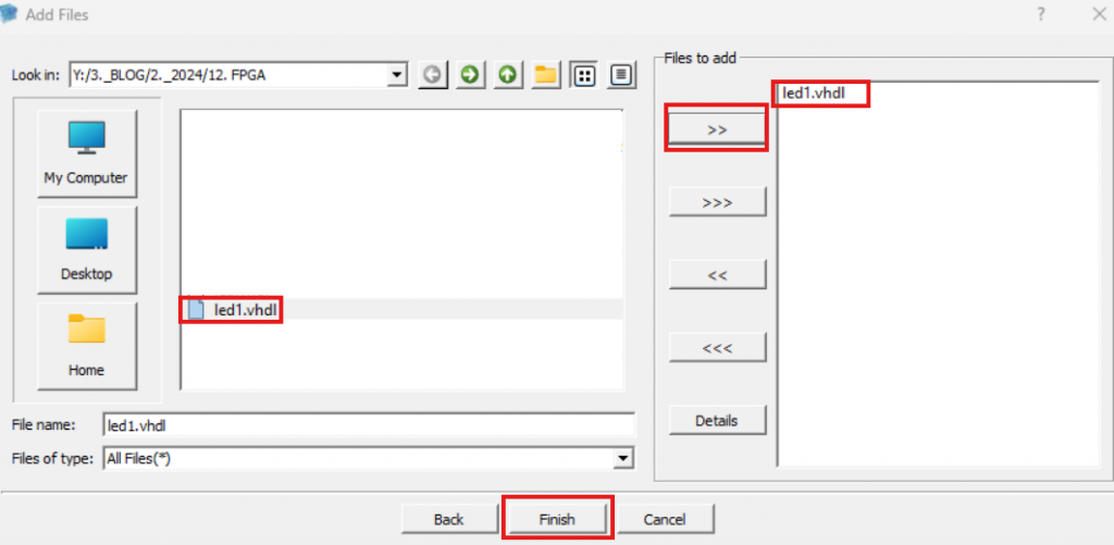
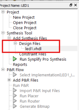
- Next I need to confirm that my VHDL file is added and showing under the Synthesis tool section
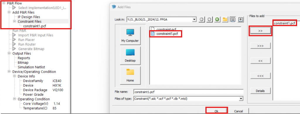
- Next, expand on P&R Files
- Right click on Constraint files
- add the .pcf file
- Right click on Constraint files
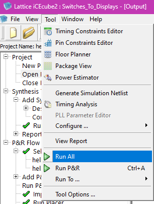
- Next go to Tool tab – and hit RUN ALL
Once the run is completed connect the FPGA and launch Diamond Programmer
Select the following:
- Device Family – iCE40
- Device – HX1KDouble click on Operation
- Change the access mode to SPI Flash Programming
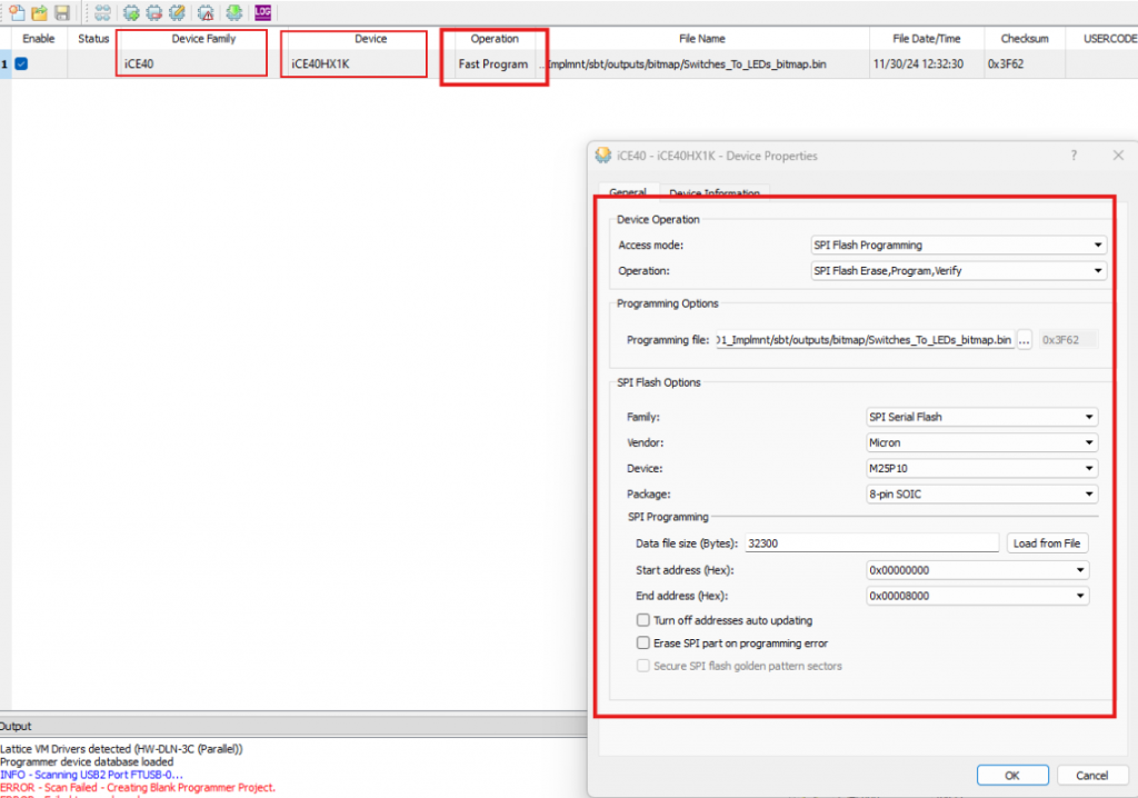
Change the access mode to SPI Flash Programming
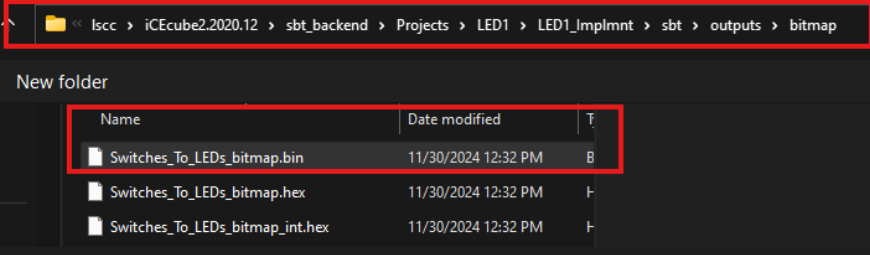
On the File name: follow the path below and select the .bin file
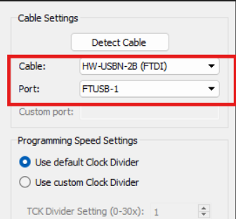
On the cable settings I make sure to select the FTDI cable and choose port 1
- Once this is done click on the Design menu and select Program
- If the programming fails change the port cable from 1 to 0
Once the operation is successful, I can test the board.

Conclusion
It worked! The LEDs blinked, and the 7-segment display cycled through “HELLO.” This experience helped me understand the basics of FPGA programming and the steps involved the in bringing an idea to life. I’m excited to explore more advanced FPGA concepts in the future!
This blog marks the beginning of a series focused on using FPGAs for offensive and defensive cybersecurity topics. I hope you enjoyed reading and found it insightful. Stay tuned for more projects, and thank you for joining me on this journey!
Wishing you Happy Holidays!
~Izzny~